Welcome to Reventech Solutions Complete EDA Engineering Solutions

Reventech Solutions set up in the year 2010 has been successful in achieving the clients satisfaction and admiration through its dedicated efforts by Engineering team in bringing out best of services. Within a short span of time it has achieved many a milestones in providing EDA services to our distinguished clientele.

Reventech solutions has been successfully achieving the clients satisfaction and fully dedicated by engineering team to bring out best of services. Our Company providing complete EDA Solutions in the fields of electronics engineering with the sole aim of fulfillment of customer’s requirement with value based quality design in the global Environment. We have been providing Hardware and PCB design services for both public and private sector in India within a short span of time. Our Engineering Team works 24*7 and provides services In-House as well as On-site as per the client’s requirement.

PCB Designing

Having over 13+ years of experience in designing PCBs, We have worked across different domains for Top OEMs. With our in-depth understanding of the materials and manufacturing process, we can provide with “First Time Right” Designs significantly reducing the time to market

Simulation (PCB Analysis)

Pre and Post layout signal integrity solutions are provided to have a better understanding of the functionality of the board regarding Time delays, Cross Talks and etc. before sending to the actual fabrication process using SI tools.

  1.    Signal Integrity
  2.    Power Integrity
  3.    Thermal Analysis
  4.    EMI & EMC Analysis

PCB Manufacturing

Tied up with various local and International manufacturing vendors for the supply of PCBs from the Commercial to Mill grade quality.

  1.    In House Manufacturing
  2.    Security Of DATA
  3.    Proper QC Methods
  4.    Strict NDA Process.

PCB Assembly

Our company has streamlined its production process by implementing in-house PCB assembly capabilities, ensuring greater efficiency and quality control.

  1.    In House PCB Assembly
  2.    From Prototype To Production
  3.    End To End PCB Assembly Solution
  4.    Team Of Professional
Blog and Social Media Section?

Reventech Solutions Complete EDA Engineering Solutions

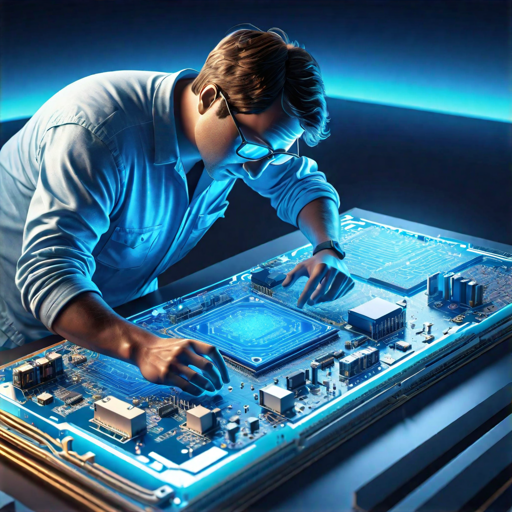
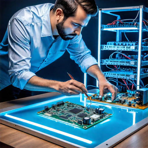
Step by step process to design high speed Printed circuit board.

PCB designing is the most important steps to develop successfull product. To design a pcb that would be efficient and compaitible with the product is the vital...

Some most used PCB designing software.

There are some PCB designing software and tools tat are used to design most effective PCB that contains multiple layers. The right tools helps to achieve it...

End To End EDA Solution.

PCB designing is the most demanded steps for the product manufacturing. It is important steps. Let us just find out the some more technical terms here ...

PCB Layout Job

8000+

PCB Analysis Job

1500+

Team Of Professionals

50+

Years Of Experience

20+

Experienced Team

Our team of EDA professionals brings a wealth of knowledge and experience, guaranteeing top-notch solutions and insights for your designs. Expert Guidance, Seamless Solutions, Navigate the complexities of electronic design effortlessly with our team of seasoned experts. From schematic creation to layout optimization, our comprehensive EDA solutions cater to every stage of your project, ensuring efficiency and precision at every turn.

THERE ARE MANY VARIATIONS

The Process That Ensures Client Satisfaction

1.

Schematic Capture & Symble Creation

We communicate with client to understand the requirement and ensure proper Schematic Capture & Symble Creation. We ensure client satisfaction and so multille time of reviews takes place.

2.

Library Creation & Placement

This is most important process and on the basis of symbol creation we proceed for the library creation.

3.

PCB Routing & Length Matching

This process increase the efficiency of the PCB and so we do it properly with perfection.

4.

Quality Check

We follow proper check list to reduce human error and ensure the design should be perfect and proper.

5.

Gerber Generation

This is the one step back process before going for manufacturing and we do dry run before giving for bulk production.

6.

PCB Manufacturing

We have inhouse machines for the PCb Manicaturing.

7.

PCB Assembly

We have well trained staff that Assemble the PCB in right way before making it functional.

IF YOU ARE GOING TO USE

Recent Reviews From Our Customers

Our Commitment to Excellence

At Complete EDA Engineering Solutions, we believe in setting new standards for innovation and precision in electronic design. Our mission is to empower businesses, startups, and individual designers with tailored EDA solutions that drive success. With a focus on customer satisfaction and a passion for cutting-edge technology, we bring a fresh perspective to every project.